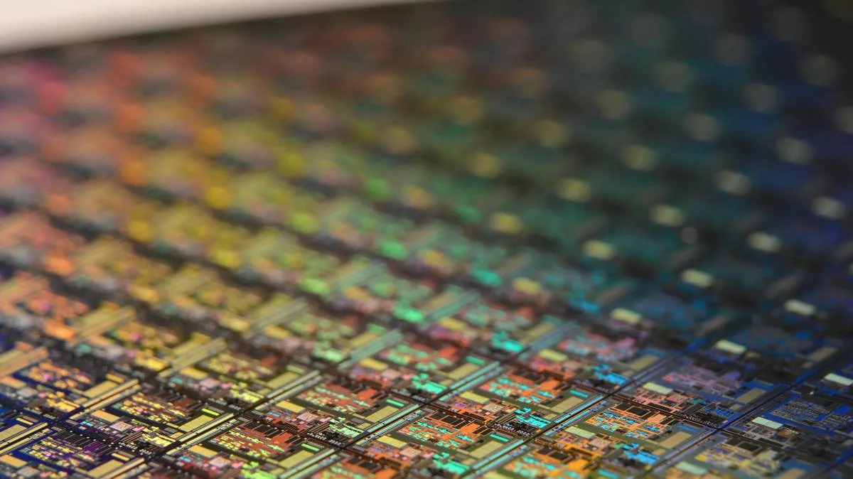
A PCB (printed circuit board) is a component that connects other electrical components together. As you can probably imagine, designing a printed circuit board isn’t easy, and requires a lot of precision to do correctly. Just one small mistake can lead to inefficiencies or problems with the end product. In this article, we’re going to take a look at the most common mistakes designers make with PCB. Have a read through, and see if you’re guilty of any of the following. If you are, you can take steps to correct them going forward.
1. Choosing a Poor Design Tool
There are a lot of PCB software options available to designers, but not all are as good as each other. Not only can choosing a poor design tool lead to increased delays in the design process, but it can also cost you money. Altium have a great low-cost PCB software which enables designers to quickly design and build advanced layouts effortlessly. The streamlined interface and workflows can be fully customized to your design team’s needs as well, making it ideal for those who have numerous designers working on one project.
2. Following Poor Layout Techniques
With the general public now expecting small, fast devices, PCB designers are required to come up with complex designs which contain all of the electronics in a narrow area. This also often means that they have to use smaller components than they usually would to get everything to fit. If you follow a poor layout technique, you are going to have constant problems, both with overheating and efficiency. You may even find that your design does not work at all. Make sure to research good layout techniques and follow them properly.
3. Lack of Communication Between Teams
Multitasking, stress and fatigue are three factors that can decrease productivity in PCB design. On top of that, they’re also the three factors that can lead to a lack of communication within design teams, which can lead to increased design costs and the need to extend timelines. One way to eliminate this is by letting the design team know exactly what is expected of them. Ensure everyone knows what their job is and that they all communicate regularly. Also, make sure that everyone knows your expected timeline for the design and that this is achievable; this will help to keep motivation high and decrease stress.
4. Failing to Back Up Their Work
Because of the intricacies of PCB design, different types of software are often used during the design process. However, this often leads to designers moving ahead without backing up their work correctly. The issue with this is not only lost time, it’s the risk of overwriting work that has already been completed. It is therefore incredibly important that designers regularly back up their work. In addition, if anything does happen to the file you have saved, a backup will be able to restore the project to the point where it last worked.
Can you think of any additional mistakes common with PCB? Let us know in the comments.